個人積分:1620分
文章編號:92539034


個人積分:16724分
文章編號:92539107
游戏脑力 wrote:
一直在讲MT...(恕刪)
你要不要找一下相關課程
台灣這通常叫 電腦概論
大陸叫啥 沒研究

如何降低 積體電路(例如處理器)運作時的功耗?
為了節省電量,可以做兩件事。
透過完全關閉子系統(核心或其他資源,如時鐘或快取)的電源
(從而降低電壓,將其降至零)來消除子系統的功耗
或者
透過降低子系統和/或整個處理器的電壓和/或頻率來降低功耗
第一個很容易理解,如果你關閉電源,就不會消耗任何電力。
第二點要多解釋一下。 積體電路(例如處理器)的功耗與頻率成線性比例,與電壓成二次比例。
P ~ fV²
而且,電壓和頻率並不是獨立的,似乎呈現線性關係。
更高的(序列/串行)性能需要更高的頻率和更高的電壓,因此對功耗的影響更大。
降低電壓/頻率的同時也會降低運作溫度,
這些對於減少半導體器件的漏電 皆有正面效益
可以進一步降低功耗或增加續航力
舉個降低學習門檻的例子
你可以把處理器看做各種不同的房子或建築物
內部有許多大小不同的房間(子系統)
剛開始,只有一個總開關
Edit...

個人積分:1620分
文章編號:92539845
相關專利在 Arm 手上。
👇👇👇
1️⃣ 关于低功耗岛(Low-Power Island)和 MTCMOS 的关系
低功耗岛(LPI, Low-Power Island) 是处理器设计里用来让一部分核心或逻辑模块在不唤醒主计算单元的情况下运行的结构。
MTCMOS(Multi-Threshold CMOS / 多阈值电压 CMOS) 是一种实现低功耗设计的技术,它可以在芯片局部关闭电源或降低电压,从而减少静态功耗(漏电)。
🔹 关系分析:
LPI 并不严格依赖 MTCMOS。它是一种“功能/拓扑概念”,核心思想是隔离和可控上电。
实现低功耗岛可以通过 MTCMOS,也可以通过其他电源门控(Power Gating)、分区供电、电压域隔离等方式。
换句话说:没有 MTCMOS 并不等于“没有低功耗岛”,只是 MTCMOS 是其中一种高效手段。
✅ 结论:
第一句 不完全正确,MTCMOS 是实现低功耗岛的一种常用技术,但不是唯一条件。
2️⃣ 关于相关专利在 Arm 手上
Arm 的确有一些低功耗管理、分区电源控制、Power Gating 等专利,尤其在移动 SoC 设计中广泛授权给厂商。
但是 低功耗岛不是 Arm 独有概念,Intel、AMD、Qualcomm 等公司都有类似实现,并有自己的专利。
✅ 结论:
第二句 也不完全正确,Arm 拥有部分专利,但“所有相关专利都在 Arm 手上”是错误的。
🔹 综合判断
说法 正确性 说明
低功耗岛必须有 MTCMOS ❌ MTCMOS 是实现手段之一,但可用其他电源门控方案
相关专利都在 Arm ❌ Arm 有部分专利,但低功耗岛实现有多家公司专利
💡 补充说明:
Intel Meteor Lake / Lunar Lake 的低功耗岛就用 独立电源域 + EMIB + E-core 集群隔离,不一定严格依赖 MTCMOS。
Arm 的 big.LITTLE / DynamIQ 架构中,低功耗岛通常结合 MTCMOS + DVFS(动态电压频率调节) 来实现。
👇👇
不要硬编谎言好吗?
個人積分:16724分
文章編號:92540209
個人積分:16724分
文章編號:92540703
個人積分:16724分
文章編號:92541152
游戏脑力 wrote:
不要硬编谎言好吗?
只看AI摘要,不做資訊查證比對
指正後還一直跳針,扣人帽子
那就別怪大家總是對你不客氣
同樣我用google AI摘要
big.LITTLE 專利主要是指 Arm 公司開發的異質運算架構,它將高性能的「big」核心與高能效的「LITTLE」核心結合,以實現不同工作負載下的功耗與效能平衡,並透過行程排程(Process Scheduling)來動態調度任務,目前 AMD 和 Intel 等其他公司也有相關的混合核心架構技術與專利,目的是為智慧型手機、平板等行動裝置提供更長的電池續航和更佳的效能。
big.LITTLE 核心技術核心概念
異質架構:整合兩種不同特性(效能與功耗)的核心。
任務調度:將繁重任務交給大核心,輕量任務交給小核心,閒置時關閉核心以節省電力。
應用:適用於智慧型手機等需要長時間待機與瞬間高性能的裝置。
專利與發展狀況
Arm 開創:Arm 推出 big.LITTLE 技術,並擁有相關的專利,是該領域的先驅。
AMD 跟進:AMD 積極佈局類似架構,並申請了相關專利,顯示其在混合處理器領域的野心。
Intel 布局:Intel 採用了類似的混合架構(如 Alder Lake),與 big.LITTLE 概念相似,追求大小核的結合。
排程方法:專利內容還涵蓋如何智慧地在不同核心叢集間切換與調度,以達到最佳能耗比。
為何重要
智慧型手機使用者對效能與續航的雙重需求,催生了 big.LITTLE 這樣的創新。
該技術超越了傳統的製程和電源管理,解決了行動裝置設計中的核心矛盾。
總結來說,big.LITTLE 是一種結合大小核心的處理器技術,Arm 擁有其原始專利,而 AMD、Intel 等也發展出自己的變體和專利,共同推動了行動處理器的功耗與效能發展。
本組態組態式在2011年10月ARM發表Cortex-A7時首次對外公布,Cortex-A15也能夠與這個架構相容。[3]
2017年5月,ARM發表DynamIQ取代big.LITTLE


更新1
Arm 的 big.LITTLE 算是引領潮流了,傳繼 Intel Alder Lake 後 AMD 也將在 Zen 5 採用大小核設計
更新2
Arm 在 2011 年推出以兼具能耗與效能的 big.LITTEL 大小核設計,而intel 在2021 年 10 月 27 日發布的第12代Alder Lake才「正式」支援**,從兩家的商業合作及intel對arm專利的向前引用數量來看(業界第一而且是第二名IBM的約一倍),授權不成問題,依照intel的尿性,頂多改個名字包裝淡化技術來源,也真的改了
 ,那為什麼拖這麼久?
 最大的問題點在於就算有專利授權,arm的big.LITTLE也是intel一時無法複製的系統架構。最主要的是x86本身的CISC架構(複雜指令集)尤其是其架構下的SIMD指令,在大小核下容易有效率不彰及資料一致性的問題。必須修改實現方式及建立相對應的機制。修著修著沒法像arm那麼異構且靈活,至少大小核指令集要統一,進一步加劇x86指令集尤其是AVX512 版本的碎片化,單從Cannon Lake 開啟的AVX512之亂就可以看的出intel在製程落後的情況下,產品開發是多麼的混亂+趕鴨子上市,為日後13/14代 縮缸 埋下了「呵呵一點都不奇怪」的伏筆,直到距離PTL正式亮相約20日的今天,仍在各種陰暗的角落,好像永遠對著你笑,笑得你心裡發寒

** 其實在Alder Lake之前還有一個類似LNL的多技術試驗田— Lakefield(2019年
堆疊了「1大4小核心」的10nm製程(P1274)運算晶片、22nm製程(P1222)系統I/O晶片和PoP(Package-on-Package)封裝的DRAM記憶體。
大核心採用了Core線的Sunny Cove核心,小核心採用了Atom線的Tremont。同樣藏著一般情況下不能用的AVX512。是截止目前X86中唯一一個同時面向高端和極低功耗設計的SoC。它的設計甚至可以說是X86迄今為止最為大膽的,也是Intel後續處理器的預覽版本。
X86大小核的首發+ Foveros 3D Chiplets設計,成本高且性能差,市面幾乎看不到太過小眾,實驗性質濃厚。
故我內文寫Alder Lake「正式」支援,這也是官方說法。但初期關閉效率核心(E-Core)的才能開啟AVX-512,仍至於之後直接將處理器中的保險絲熔斷徹底禁用,最後強制主機板商刪除 較早處理器可從 BIOS 啟動 AVX-512 指令功能的做法,甚至在今天可以在官方「支援知識庫」找到:
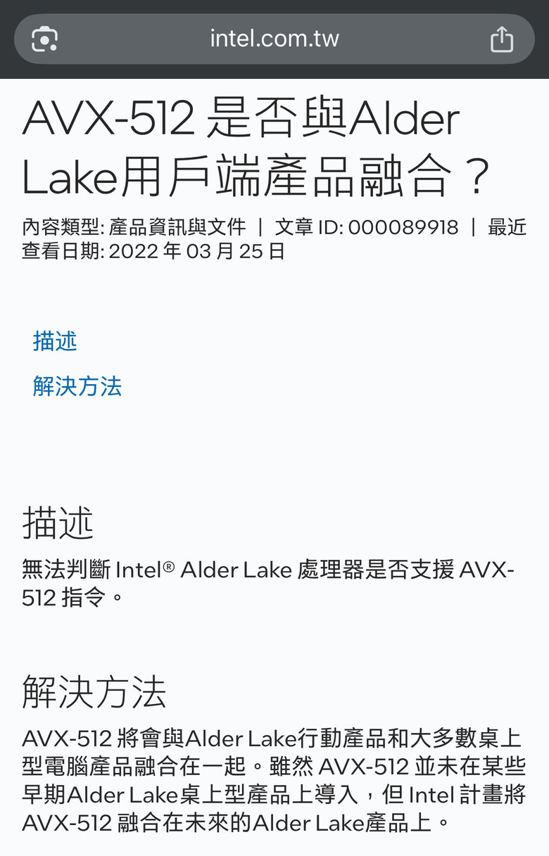

讓我對於所謂的「正式」支援 存疑。
當初為了吹AVX512在自家10nm扛不住的情況下在消費端硬上,後面又為了行銷上打核(數)戰在Alder Lake上遮蔽它
說著說着,AVX512在AMD ZEN上取得成功,又讓intel後悔,打算在未來恢復,真是夠了
https://technews.tw/2023/05/03/support-avx-512-instruction-cpu/
https://www.phoronix.com/news/Nova-Lake-Does-AVX10.2-APX
整個AVX512發展屎,在Intel上面就是一地雞毛,由於篇幅實在太長,想打發時間可以自行搜索,過程”精彩”可以輕易找到,更新2技術引入及正式支援大部份觀點應該只有這裡找得到,對於big.LITTLE講著講著,莫名其妙變成吐槽AVX512,我也是挺
 的…
的…
個人積分:16724分
文章編號:92542670
專家示警「危險訊號」,英特爾怎麼說
有消息指出,陳立武的投資行為已多次引發潛在的利益衝突,《路透》報導,陳立武曾多次推動英特爾考慮收購他本人投資或任職的新創公司,包括與 Meta(META-U )爭搶 AI 晶片新創 Rivos 的競標案,以及人工智慧(AI)公司 SambaNova。
而這些公司恰好都有陳立武的個人投資,讓陳立武近日再次捲入新的爭議風波。
Intel RMA 13900K 風波 用戶控訴原答應退款被反悔, 只能換新
他表示自己向 Intel 申請 i9-13900K 的 RMA,起初 Intel 已明確表示可以退款。但在他依照流程提交所有資料後,Intel 卻突然變卦,理由是「購買證明驗證失敗」。
問題是,Superino 提供的發票是來自知名通路,並非可疑來源,讓他完全無法接受官方的態度轉折。
為維持電腦運作,先自費換新 CPU 結果卻換來退款遭拒
英特爾引爆國安危機?
傳與被美制裁公司合作 專家:防堵政策有重大漏洞
A19 和 A19 Pro 的晶片尺寸比 A18 和 A18 Pro 小 10%,同時卻擁有更高效能的核心、更大的 GPU 和 E-Core 面積——蘋果是如何做到的?
在遊戲 燕雲十六聲,A19 Pro 的穩定性優於驍龍 8 Elite Gen 5,初步對比也顯示,iOS 移植版在高解析度下運作順暢。
個人積分:16724分
文章編號:92545249
Nova Lake-S CPUs will be Fabbed on Intel’s 18A Process; Team Blue to Focus on High-end SKUs
我是看不出來,有這個意思
Barclays銀行第23屆全球科技年會 英特爾副總裁John Pitzer對談紀錄
Thomas O'Malley
Barclays Bank PLC, Research Division
You're leaning on some outside IP today. I think most recently, last week, you talked about 70-30, which you reiterated from kind of the earnings call. As you move forward, where is that headed with Nova? Can you talk about splits there?
John Pitzer
Corporate Vice President of Corporate Planning & Investor Relations
Yes. So when you say IP, it's really externally sourced wafers from external foundry suppliers. Yes. So roughly speaking, about 30% of the wafers that we get today are externally sourced. We've talked about Panther Lake starting the process of bringing more wafers internally. And so as you think about kind of our external strategy on the client side, it really started with Meteor Lake a couple of years ago, where 1 of the 4 tiles was outsourced. That was accelerated both with Arrow Lake and Lunar Lake, which is today our leading-edge parts on notebook desktop for Arrow Lake and notebook for Lunar Lake.
And those are at least on the compute tiles -- sorry, the logic tiles are 100% outsourced. We still do a lot of the base die and advanced packaging internally, but most of the active tiles are externally sourced. What we've said with Panther Lake is to the extent that Arrow Lake and lunar are 100% outsourced, about 70% of the tiles that we need for Panther Lake will be coming back in-house, which is a positive relative to filling fabs and driving better profitability.
I will remind people, Panther Lake is only a notebook part. As we move to Nova Lake, Nova Lake will cover the full PC stack of notebook and desktop and bring even more wafers back. And so we've kind of got a trajectory now today where we're going to be bringing more internally. Having said that, I'll also remind you, as we navigate this tight supply situation, we are shifting more of our internal capacity away from client towards server to serve that market. And we are leaning a bit more heavily on some of our external suppliers on the foundry side around Arrow Lake and Lunar Lake to augment some of the volume that we're shifting internally towards servers.
這些公開發言,通常是盡可能的修飾措辭、報喜不報憂,仍有一些值得玩味的地方。例如:
On 18A, listen, our first product out on 18A is Panther Lake, it's internal product for PCs. We had committed to getting our first SKU out by end of year. The good news is we've done that. ...... we're shipping, it's really CES, which is the launch event.
I think when Lip-Bu joined the company in March, he was clearly unhappy with where absolute yields were.
I think he was even more unhappy that the progress on 18A yield was kind of half hazard. I think as you fast forward to today with a lot of work that Naga, Lip-Bu and the teams have done. I'd say we've gone from unhappy to unsatisfied because we'll never be satisfied with where our yields are on 18A,
I think Again, when Lip-Bu did his deep dive on 18A yields and was not happy. I mean the first thing he told the team to do is why are we engaging external customers with a product that's not good.
I think in general, it was really incentivizing the teams and quite frankly, leaning more heavily on suppliers. I think Lip-Bu -- one of the reasons why the board hired Lip-Bu is because he has a tremendous network within the semiconductor ecosystem. And on day 1, he did something that we've never done, which is share our yield data with external suppliers, and I won't mention names, but they've been extremely helpful. And I think Naga has put a huge focus on this as well. And I think that the improvements we've seen as we've gone throughout 2025 are a reflection of those efforts.
The 3 I would point to is during 18A, in the definitional phase of the node, we weren't really engaging with the external world. We were really only engaging with Intel products as the internal customer. And all of the decisions we made on the transistor level was really to optimize for them.
And it wasn't really to the development phase that we started to get some true feedback from external customers. In 14A, in the definitional phase we are engaged with external customers. And what that really means is we're getting earlier, more and better feedback and feedback that can actually influence how we develop the node a lot quicker. So that's absolutely helping us.
The second thing that's helping us is I tend to tongue in cheek say that we didn't learn how to spell PDK until about halfway through the 18A node. And we had a lot of growing pains in making sure that our PDKs were industry standard like. And we continue to miss the mark on 18A. We were late with our 1.0 PDK. When we finally got it out, if you did channel checks, some customers would say, it really wasn't a 1.0 PDK. The good news is we took all of those sort of lessons and we forward fed them, quite frankly, both into the 18AP PDK, which is maturing nicely, but also on the 14A PDK.
Yes. So our CapEx guidance for this year on a gross basis is at $18 billion. I would say, at the end of Q2, we were emphatically saying it was going to be down next year. I think given some of the tight supply we have today, I think directionally down is still right. I'm not sure we're as emphatic as we were. And there's a couple of things to keep in mind. As we -- especially as we start to get into early next year given the lead time of actual -- from spend to ramp, most of next year's CapEx is really about 2027 capacity, not about 2026 capacity.
Before I answer that, one last point I want to make on CapEx for next year, we are not prebuilding for external foundry. And so when we win an external customer, we will need to come back to the market and increase our capital spending plans. Now there's probably 2 phases to that. I think the initial tranche of 14A customers, we should be able to support out of Arizona, which will be an increase in CapEx, but not a meaningful increase in CapEx. The more meaningful increase will come when we have to start accelerating Ohio.

個人積分:10930分
文章編號:92545888
純論產品本身PTL在2026中筆電上還是有吸引力
可惜intel的問題不是在產品規格上
而是規劃及排程混亂,還有執行力等更高層面的問題
個人的看法是由於市場慣性,對手又因為分不出多少資源顧到2026的消費級產品上,筆電這塊在2026還是intel的地盤
但intel的戰場不只筆電,而是含括桌機.工作站.伺服器,網路硬體相關
(大概因為之前有各方注資,他們又打算不賣了要自己玩,先前市場跌勢反應出各金融投資對intel非核心資產分割不果決的失望)
還有近幾年熱錢所在的AI相關建設等落後市場各競爭者
加上新CEO在多起併購案件上有介入自肥的疑慮,導致基礎仍顯得不太穩固,未來展望大概沒他們自己說的那麼明亮
個人積分:16724分
文章編號:92563056
2023 年末,ASML 向英特爾交貨了首套 High-NA EUV 微影曝光設備,型號為 TWINSCAN EXE:5000 的系統。英特爾將其做為試驗機,並於 2024 年在美國俄勒岡州的 Fab D1X 晶圓廠完成安裝。之後,該晶圓廠成為英特爾半導體技術研發基地,進一步研發使用 High-NA EUV 設備的技術與產品。
日前,英特爾進一步宣布,已安裝了更新的 ASML 的 TWINSCAN EXE:5200B 微影曝光設備,這是目前全球最先進的微影曝光設備,屬於第二 代High-NA EUV,將用於 Intel 14A 節點製程上。英特爾指出,在與 ASML 的合作下,已成功證明了最先進的微影曝光設備在提供改進的精度和生產力方面的技術可行性,為 High NA EUV 微影曝光設備未來的大量製造奠定了基礎。
根據資料,ASML 的 TWINSCAN EXE:5200B 微影曝光設備在標準條件下,產量可達到每小時 175 片晶圓,但英特爾計畫做進一步調整,提升至每小時 200 片晶圓以上。新系統還在英特爾過去一年多對 High-NA EUV 微影曝光設備的使用經驗之上,提升了套準精度達到了 0.7 奈米。
英特爾表示,High-NA EUV 微影曝光設備是其晶圓代工技術中的重要能力,結合了自身在掩模、蝕刻、解析度增強和計量等相關領域的技能,達成了當今晶片所需的更精細電晶體細節。對 IC 設計來說,這帶來了更靈活的設計規則,減少步驟和掩蔽次數的能力意味著流程更簡化,良品率更高,而且時間更短。目前英特爾仍處於早期階段,但這代表著在為客戶提升效率與生產力方面取得了積極進展。
https://www.techpowerup.com/344132/intel-installs-asml-twinscan-exe-5200b-high-na-euv-machine-for-14a-node
不計其他工序
TWINSCAN NXE:3800E 每小時 可以曝光 220片晶圓
TWINSCAN EXE:5000 每小時 可以曝光 185 片晶圓 劑量:20 mJ/cm²
TWINSCAN EXE:5200 每小時 可以曝光 175 片晶圓 劑量:50 mJ/cm²