今天SeekingAlpha發佈了一篇文章(TSMC Significantly Underdelivers)
指出:
Intel晶片的電晶體密度將於2024年達到400MT,2026年達到800MT。但台積電直至2026年都無法達到300MT。也就是說2026年時Intel的晶片電晶體密度將會是台積電的3倍之多。
Mobile01裡面的半導體專業人士請評論這有沒有可能?還是又是美國人的優越感作祟?

個人積分:5153分
文章編號:85197514

個人積分:24671分
文章編號:85197934

個人積分:1922分
文章編號:85198082
個人積分:4600分
文章編號:85198434
個人積分:24671分
文章編號:85198617
Cavendish Lab wrote:
今天SeekingAlpha發佈了一篇文章(TSMC Significantly Underdelivers)
該作者的 LinkIn:
https://www.linkedin.com/in/arne-verheyde-567054153/?originalSubdomain=be
Education:
KU Leuven logo
KU LeuvenKU Leuven
2016 - 2021
去年大學剛畢業的小朋友,誰想信誰就傻了。。。。。。
工作經驗:
Experience
Freelance Journalist
VentureBeat · FreelanceVentureBeat · Freelance Nov 2021 - Present · 8 mosNov 2021 - Present · 8 mos
Analyst
Seeking Alpha · FreelanceSeeking Alpha · Freelance Jan 2020 - Present · 2 yrs 6 mosJan 2020 - Present · 2 yrs 6 mos
Freelance Journalist
Tom's Hardware · FreelanceTom's Hardware · Freelance Mar 2019 - Mar 2020 · 1 yr 1 mo
倒是手上的持股蠻有趣的,都是我這幾年曾經的主力持股。


個人積分:15029分
文章編號:85198786
台積最大的關鍵是毛利率,和半導體需求狀態。
TSMC 的問題是毛利率能不能拉高,eps 拉高。
最重要是配息能不能調高。一季要配到 4元,股價才有機會上衝。
500元股票,16元配息,殖利率才能過 3%
台積年底量產3nm, 密度 310 MT
TSMC的 3nm 是第一個達到 300 MT 製程,領先 第 2,3 名一大段距離。
2025 2nm 密度約 400 MT
三星即將試產的 3nm,密度200 MT.
和 TSMC 5nm 的 185MT 接近,密度應該打不過 TSMC 的 4nm
且 三星的 良率跟 發熱,是有目共睹的低劣。
所以三星已經輸給了 TSMC.
三星 3nm 連 TSMC 4nm 都打不過,更不用談 TSMC 3nm
intel. 目前最好的 10nm,密度是 106MT.(106MT 是 Scotten 的計算,簡報常用數字是 100.8MT)
跟 TSMC 7nm 的 102 MT 相近。
完全輸給 TSMC 5nm 的 185MT,
更不用比 TSMC 4nm,3nm.
intel 計畫2022/2023/2024 分別量產 4nm/3nm/2nm
intel.的 schedule 完全是畫大餅,感覺應該是申請經費用,實際上是不太可能,
依照以前的記錄,都是嚴重 delay.
而且要一年一個世代,不太可能。
2022/2023. 的 4nm/3nm, 密度比 TSMC 3nm 低,
至於 2024/2nm,密度應該也沒比 TSMC 3nm好太多,
但問題是 schedule ,良率,產能,耗電 都是大問題,所以聽聽就好。
我看 頂尖專家 Scotten Jones的圖表,intel 2nm (20A) 看似只有比300 MT 好一點。
--------------------
(實際計算 7nm 106MIT * 1.35 *1.09 * 1.6 = 250MT)
上面黃色誤植,重新計算後,接近的數字應該是
100.8 * 1.8 * 1.09 * 1.6 = 316 MT
----------------------
效能方面,intel 倒是不錯,沒輸給 TSMC, 因為是PC 用,可以大電力比較耗電,也可以加風扇散熱。這個市場,本來就是 intel. 的專長。
台積明年3nm的客戶,intel 可能是最大客戶。
intel. 還是要靠 TSMC 的 3nm , 才能擺脫 AMD.的追趕。
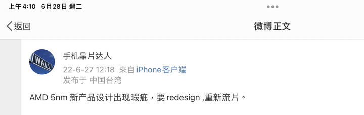
AMD 聽說最近量產的 5nm. CPU出包,需要重新流片。
這有點慘,需要花大錢,花時間。
Scotten Jones 原文:
-----------------------------
Our view from now to 2025 is as follows:
2022 – Intel 4nm process, Intel’s first EUV use with a 20% performance improvement over 7nm. Intel had formerly talked about a 2X density improvement for this generation but is now just saying a “significant density improvement”, we are estimating 1.8X. Samsung 3nm will likely be for internal use only with a 1.35X density improvement, 35% better performance at the same power and 50% lower power at the same performance. The density improvement is not very impressive but the performance and power improvements are, likely due to adoption HNS. TSMC 3nm is FinFET based and will provide an ~1.6X density improvement with 10% better performance at the same power and 25% lower power at the same performance.
2023 – Intel 3nm process with 18% better performance, denser libraries and more EUV use. We estimate a 1.09X density improvement making this more of a half node. Samsung 3GAP should be available to external customers and TSMC 3nm parts should appear in iPhones.
2024 – in the first half Intel 20A (20 angstrom = 2nm) process is due with a 15% performance improvement. This will be Intel’s first HNS (they call it RibbonFET) and they will also introduce back side power delivery (they call this PowerVia). The backside power delivery addresses IR power drops while making front side interconnect easier. We are estimating a 1.6X density improvement. In the second half of 2024 Intel’s 18A process is due with a 10% performance improvement. We are estimating a 1.06X density improvement making this another half node. This process has been pulled in from 2025 and Intel says they have delivered test devices to customers.
個人積分:3606分
文章編號:85198799
個人積分:12252分
文章編號:85198925

個人積分:2257分
文章編號:85198951


個人積分:1636分
文章編號:85199028